Digital Sensor Characterization
A technical deep-dive into CMOS architecture and methods for characterizing sensor performance in a home laboratory setting.
1. The Architecture of Modern Capture
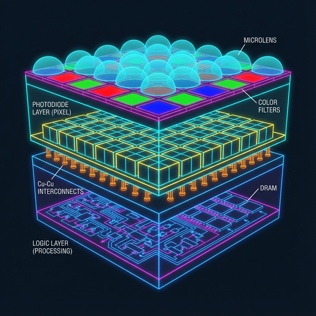
Over the past 20 years, the industry has engineered sensors for the world's most demanding optical systems—from Leica's rangefinders to Hasselblad's medium format backs. The shift from CCD to CMOS was pivotal, but the true revolution lies in the Stacked Back-Illuminated (BSI) architecture shown above.
In modern Sony sensors, we separate the photodiode layer from the logic/processing layer. This allows us to maximize the fill factor of the pixels (capturing more photons) while simultaneously using a high-speed logic process node for the readout circuitry beneath. The Cu-Cu (Copper-to-Copper) interconnects provide the high-density vertical electrical pathways needed to parallelize readout, essentially eliminating the "rolling shutter" effect in our latest designs.
2. The Photon Transfer Curve (PTC)
Decoding the Signal
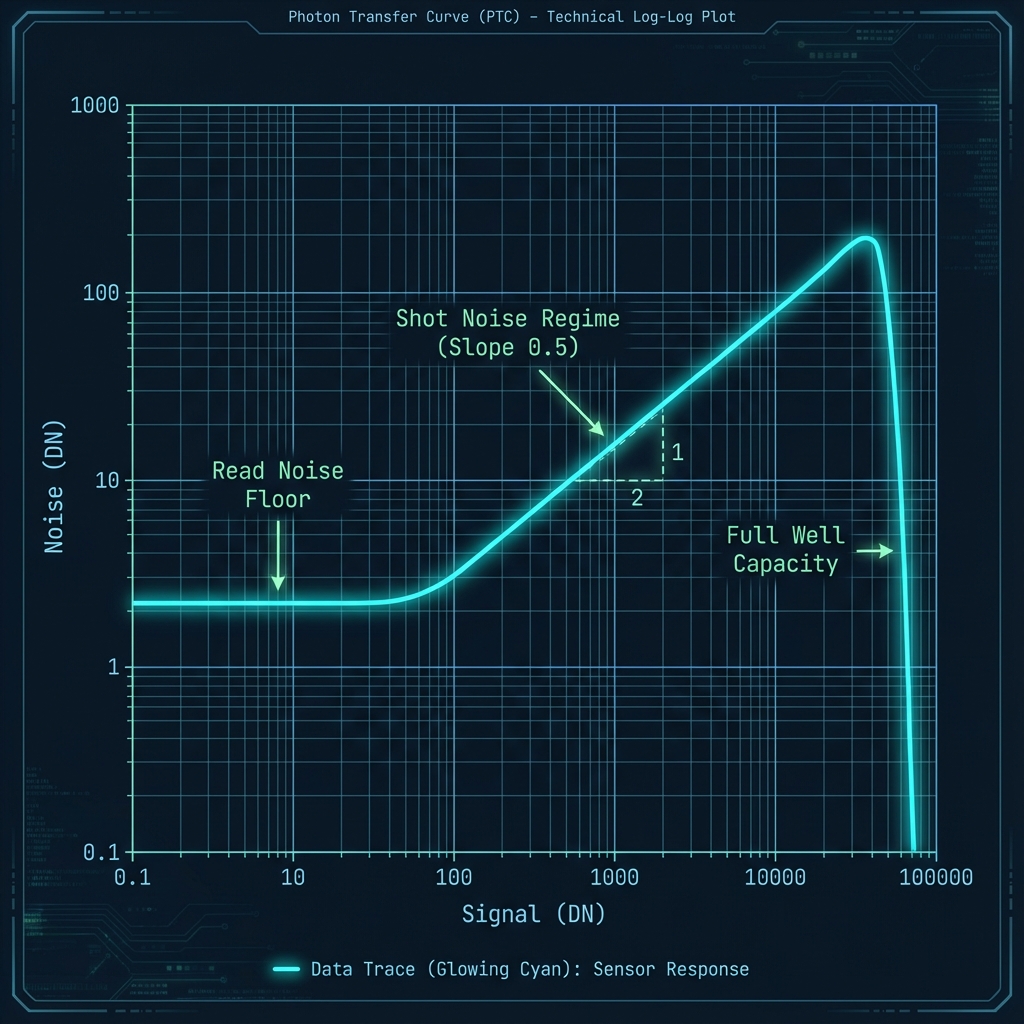
The Photon Transfer Curve (PTC) is the "heartbeat" of any image sensor. It plots the noise (standard deviation) against the signal (mean) on a log-log scale. This single plot reveals the three fundamental operating regimes of the device:
- Read Noise Regime: The flat floor on the left. This is the electronic noise inherent to the readout chain, independent of light.
- Shot Noise Regime: The slope of 0.5 (or 1/2). Here, photon statistics dominate. Noise scales with the square root of the signal ($\sigma = \sqrt{S}$).
- Full Well Saturation: The sharp drop-off on the right. The pixel is full, variance collapses because every pixel reads the maximum value.
3. Experiment: Generating Your Own PTC
You do not need a million-dollar lab to characterize your camera. You can generate a PTC using a standard digital camera capable of shooting RAW.
Equipment Required
- Camera: Must support RAW (compressed or uncompressed).
- Light Source: A stable, flat light source (an iPad screen displaying white, set to fixed brightness, works well).
- Software: specialized analysis software is best, but you can use RawDigger or write a simple Python script using `rawpy`.
Procedure
- Pair 2: 1/4000s
- ...
- Pair N: 1s (Saturation)
Python Analysis Snippet
Use the following snippet to process a pair of RAW files:
4. Interactive Simulations
Sensor architecture is best understood through experimentation. Use these interactive modules to simulate fundamental physical properties of image capture.
Sim 1: The Photon Rain (Shot Noise)
Photon arrival is a Poisson process. As light levels drop, the "rain" of photons becomes sparse, creating visible noise.
Sim 2: Dynamic Range Architect
Design your own sensor pixel. Adjust the Full Well Capacity (FWC) and Read Noise to see the theoretical Dynamic Range.